Common Failure Modes in HDI Printed Circuit Boards
Modes in HDI Printed Circuit Boards
Printed circuit boards are essential for a wide range of electronic devices from medical equipment and smart watches to satellites and airplanes. However, the intricate design of a PCB makes it vulnerable to a number of different failure modes. Some of these can be prevented, while others are inevitable. PCB contract manufacturers are tasked with meeting the demands of customers while maintaining rigorous quality standards and improving product performance, reliability and longevity.
The most common failure modes in hdi printed circuit boards include electrical, mechanical and structural issues. A thorough PCB inspection and investigation is required to identify the source of the problem. In many cases, these issues can be corrected through rework and/or repairs. A comprehensive fault isolation and root-cause analysis can take weeks, depending on the complexity of the board.
Mechanical failures of a hdi printed circuit board occur when stress and alteration cause the material to deform or warp. This can be due to vibration, thermal cycling or field conditions. Typically, these problems are difficult to diagnose without the use of a microscope or other advanced tools. This type of failure is usually not preventable, but can be mitigated with proper manufacturing practices and quality control.
Common Failure Modes in HDI Printed Circuit Boards
The mechanical failures of a circuit board are primarily caused by stresses and strains induced by the fabrication process. Various processes such as etching, sanding and wet chemical processing generate stress. In addition, mechanical cutting (V-scoring) and wet lamination can also induce distortions.
While electrical and structural failures are more common in PCBs, mechanical issues are still a significant factor in the overall quality of a board. The most common mechanical failures include elastic and plastic deformation, fatigue fracture initiation and propagation, brittle fracture and warpage.
When a Printed Circuit Board is improperly assembled or populated, the components can contact each other and interfere with the flow of electricity. This can cause faulty operation and even failure of the entire circuit board. The assembly and assembly of a PCB requires extra precision because of the miniature pads and fine pitch components used on these boards. This heightened accuracy increases the likelihood of human error, which can lead to circuit board failure.
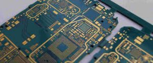
Vias, microvias and through-holes are drilled holes or cylinders that connect all layers of a PCB. HDI PCBs can incorporate laser drilled microvias, blind and buried vias and extremely fine traces. These features allow for a high routing density in the PCB, which helps to save space and reduce weight.
A PCB’s routing density can be affected by its construction, the types and amount of vias, the stack-up height and number of sequential laminations. Each of these factors can have a significant impact on the PCB’s price. For example, a 2-n-2 high-density PCB is more expensive than a 1-n-1. This is because the 2-n-2 layout uses more layers and requires more complex constructions than a 1-n-1.