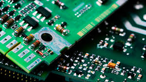
How Are Vias Filled During Circuit Board Assembly For Improved Reliability?
Circuit Board Assembly For Improved Reliability
When PCB design calls for vias to connect layers, they need to be filled with a material that is capable of effectively transferring electrical current and dissipating heat. Vias that are not filled properly can develop microscopic fractures or short circuits over long operational lifetimes. Integrating protective measures like filled and capped vias into your circuit board assembly ensures improved reliability in environments that pose moisture or mechanical stress during operation.
There are different types of vias on a PCB including through-hole, blind or hidden, and buried vias. Through-hole vias travel through the entire circuit board connecting traces on the outer layers and, if needed, on the inner ones as well. Blind or hidden vias don’t extend beyond the surface of the circuit board assembly but connect a pad on the surface to a hole in one of the internal layers. Buried vias are completely encapsulated inside the board with no visible ends on the surface and are only accessible by drilling.
Conductive fills are often used to provide the proper conductivity between the pads and holes. Metals like copper and silver are often used because they are good thermal conductors and can efficiently transfer electricity. Typically, these conductive materials are plated through electroplating. This process requires a precise plating level and can be expensive but is necessary to ensure the correct conductivity between the components and the vias on the PCB.
How Are Vias Filled During Circuit Board Assembly For Improved Reliability?
Non-conductive fills are also available for vias. These are often used to stop solder from wicking into the hole and flow down the sides of the via, which can cause poor or even non-existent connections. This type of fill can be cheaper than a conductive one and still offers adequate protection against the issues that come with solderwicking.
Choosing a suitable via filling method can significantly reduce the cost and turnaround time of your project. There are several processes for filling vias including roller coating, screen printing, and vacuum plugging. It’s important to choose a manufacturer that has experience with each of these methods and can execute them in a way that provides precision, consistency, and reliability.
Reflow soldering involves heating the PCB and components to melt solder paste, forming connections as it cools. Hand soldering is typically reserved for intricate or low-volume assembly, requiring skilled technicians to solder individual components.
A key factor in via filling is the cleanliness of the circuit board before the process begins. To avoid contamination, the PCB should be cleaned and prepped to remove any oxidation or other debris. It’s also important that the drill holes are sized correctly. If they are too small, they may not be able to accommodate the required fill materials or the plating process. For maximum reliability, PCB manufacturers recommend using larger via drill holes with an aspect ratio of 6:1 or higher. While this may not be feasible for every design, larger vias offer greater mechanical strength and better electrical and thermal conductivity.